Understanding HDI PCB and Aluminum PCB: Advanced Solutions for Modern Electronics

Today, because of rapid changes in electronics, printed circuit boards (PCBs) have a key effect on how well and how long electronic equipment performs. Because of their unique advantages and uses, HDI PCBs and Aluminum PCBs have become very popular. This blog will discuss these two kinds of PCBs in depth, including what they are, how they function, and the ways they are made.
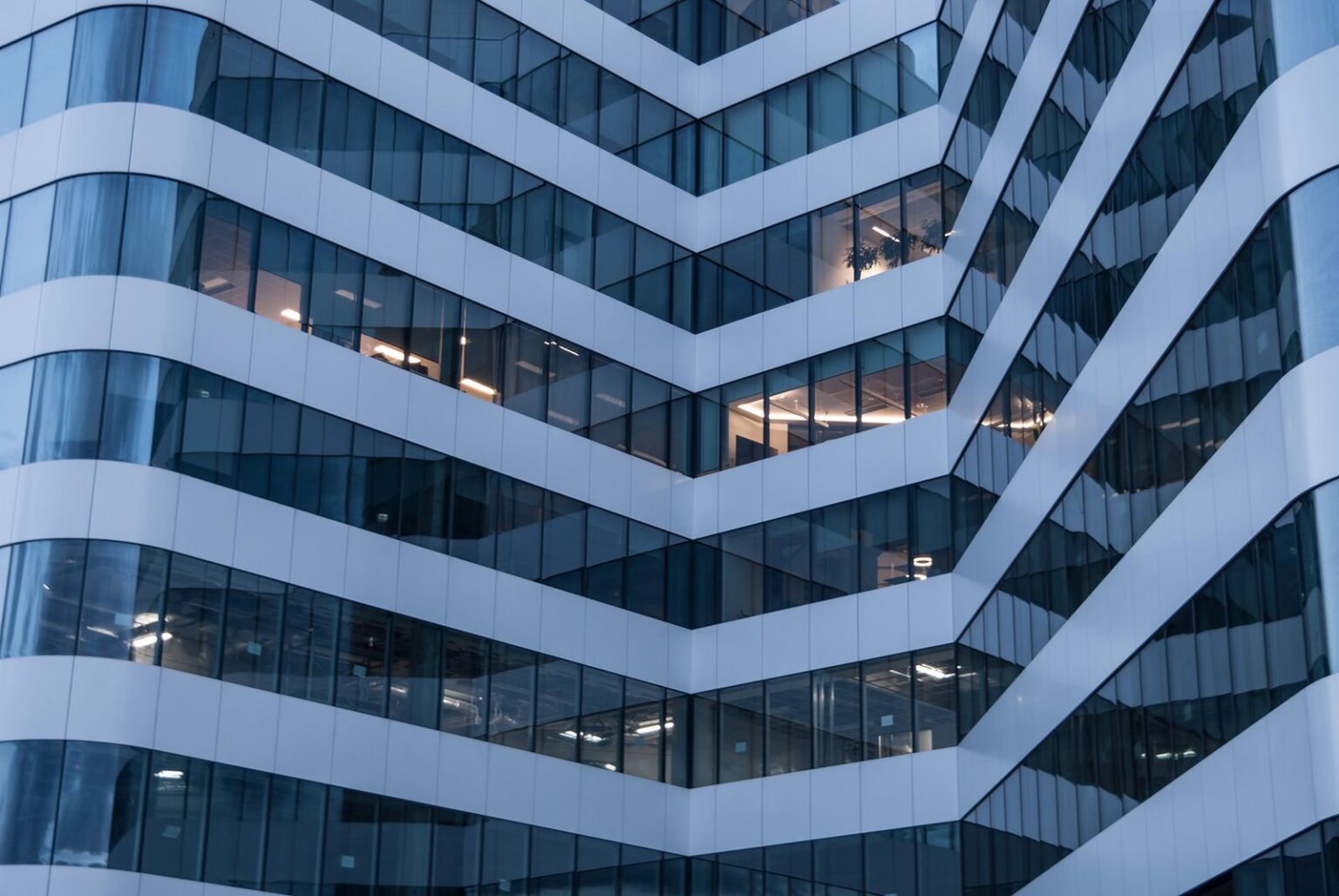
What is an HDI PCB?
A PCB that is HDI is meant to have more connections per square inch than a standard printed circuit board. Microvias, blind vias, and buried vias create room for more components and connections in less space.
PCB designers can make the newest electronic devices, such as smartphones, tablets, laptops, and communication devices, more compact as they enable faster and more complex electronic circuits. HDI technology enables high-feature devices at lower volume without compromising the supply of electricity.
Features of HDI PCBs
- Microvias and Blind/Buried Vias: They enable interconnection among different layers without consuming much extra space.
- Fine Spaces and Lines: Very fine spaces and lines can be achieved using HDI technology in PCBs for accurate signaling.
- Multilayer: Required for intricate circuits in multilayered PCB designs.
- Improved Signal Integrity: Signals can travel with minimal loss and perform effectively in high-frequency circuits.
Advantages of PCBs
There are some reasons why the latest electronics employ PCBs instead of conventional PCBs.
- Miniaturization of Products: HDI technology enables things to become smaller and lighter in weight, yet operational.
- Electrical Performance: VNTDs lead to shorter traces and minimized signal delay, interference, and noise.
- Enhance Reliability: Microvias are stronger and reduce the likelihood of certain components failing.
- Flexibility in Design: Enables the integration of complex circuits and other elements.
Advantages of these are greatest in use industries such as aerospace, medical devices, consumer electronics, and automobile, where space, weight, and performance are tightly managed.
What is an Aluminum PCB?
PCBs or metal-core PCBs (MCPCBs) refer to copper-free printed circuit boards that use a base material of aluminum rather than the common fiberglass. The metal core possesses good thermal conductivity, so these PCBs are best applied where heat needs to be dissipated.
PCBs find extensive application in LED lighting, power electronics, car electronics, and many other areas where reliability is an absolute requirement. The aluminum substrate enables easy heat conduction away from delicate circuits, thereby improving device reliability and lifespan.
Structure of PCBs
A standard PCB consists of three layers:
- Circuit Layer: The surface layer on which copper traces are imprinted.
- Dielectric Layer: Electrically insulating but thermally conductive, the layer insulates the circuit from the metal base.
- Metal Base: Inexpensive aluminum, for mechanical support and heat conductivity.
Overview of Manufacturing Process
HDI PCB Manufacturing
Fabrication of PCB is a sophisticated process that entails laser drilling for microvias, sequential lamination to construct multilayer boards, and fine-line photolithography for trace patterns of high accuracy. Due to features being very tiny in size, verification and inspection of quality are the most significant aspects to impart functionality and reliability.
Aluminum PCB Fabrication
PCB manufacturing consists of etching, copper foil lamination, and dielectric layer lamination on the aluminum substrate to fabricate the circuit. The most challenging aspect here is maintaining good adhesion between the layers along with high thermal conductivity, without compromising electrical insulation.
Challenges in HDI and Aluminum PCB Manufacturing
Though both possess their advantages in most aspects, there are certain drawbacks in their manufacturing processes. In the case of HDI PCBs, which are very small, like microvias and ultra-thin traces, quality machinery and quality control are necessary. Even a minute misalignment or defect at this very small level can cause a malfunction in signal transmission. Also, HDI boards typically have more than a single layer, so they are more complex and expensive.
Aluminum PCBs also present problems concerning bonding the dielectric layer to the metal substrate. Insufficient bonding will cause delamination or a lack of good thermal performance. The aluminum core needs careful handling as well to prevent warping or damage during fabrication.
Environmental Considerations and Sustainability
With the electronics industry becoming greener when it is manufactured, PCBs and aluminum are both taking a hit from the trend toward green. With PCBs being heavier in material and more complex, they may be more energy-thirsty and wasteful when manufactured. Not that they need to be, but their size advantage does mean that they are less material in total resources consumed by the product, to some extent.
PCBs would be recyclable due to aluminum’s recyclability. Recyclability makes it possible for there to be fewer environmental issues compared to standard PCBs. The industry also looks into greener dielectric compounds and lead-free soldering technology for increased sustainability.
Future Trends in HDI and PCB Technologies
The future of PCBs looks bright with continued research in microvia technology, embedded elements, and flexible HDI boards. The evolution will allow for even smaller devices with higher computing power and connectivity.
In the case of PCBs, the research aims to improve thermal interface materials and incorporate cooling functions in the design so that the PCB may be optimized as far as performance is concerned for high-power applications such as electric vehicles and 5G facilities.
Conclusion
Both HDI and aluminum PCBs are essential technologies in the current electronics production, both of which are solving various problems — HDI for fine miniaturized circuitry, and PCBs for thermal management in power electronics. The selection of the correct type mainly depends on your application requirements, device limitations, and performance specifications.
Wherever you are looking for high-quality PCBs, working with experienced, established fabricators like BS Interconn Hong Kong Co., LIMITED will give you professionally engineered boards to the requirements of your project.
Frequently Asked Questions (FAQs)
Q1: What does HDI stand for in PCB manufacturing?
A1: HDI stands for High-Density Interconnect, a PCB type that uses advanced microvias and fine lines to pack more circuitry into a smaller area.
Q2: Why are PCBs preferred for LED lighting?
A2: PCBs provide excellent heat dissipation, which is crucial for LED lights to maintain brightness and longevity by preventing overheating.
Q3: Can HDI and PCBs be combined in one device?
A3: Yes, some devices use PCBs for compact circuitry and PCBs for heat-sensitive components, depending on design requirements.
Freshvoicehub