How HDI PCBs Are Redefining Modern Electronics Design
In the ever-evolving world of electronics, the demand for smaller, faster, and more efficient devices is pushing the boundaries of design and manufacturing. A significant innovation that is contributing to this transformation is the rise of HDI PCBs (High-Density Interconnect Printed Circuit Boards). These advanced circuit boards are changing the way engineers approach electronics design, offering solutions that were once considered impossible. From smartphones to wearable technology, HDI PCBs are at the heart of modern electronic devices, offering new levels of performance and miniaturization.
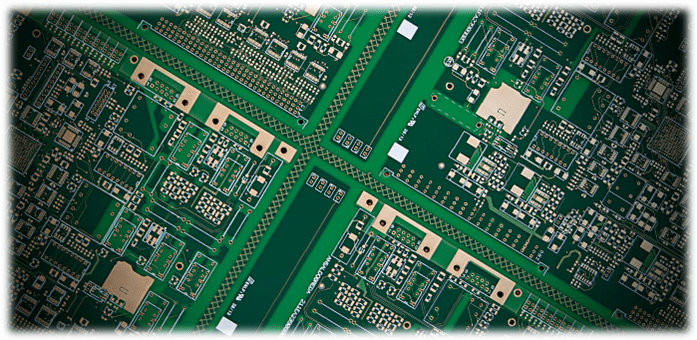
What Are HDI PCBs?
HDI PCBs are circuit boards with a higher wiring density than traditional printed circuit boards (PCBs). The design of HDI PCBs incorporates finer lines, smaller vias, and more layers, allowing for greater circuit density. This enables manufacturers to pack more components into a smaller space, ultimately creating devices that are not only more compact but also more efficient and reliable.
The technology behind HDI PCBs is built around using microvias and laser-drilled holes, which significantly reduce the space required for traditional through-hole vias. This results in a more compact and precise circuit design, ideal for applications where space, performance, and speed are crucial. In addition, HDI PCBs are typically made with high-quality materials that improve thermal management and signal integrity, which are vital factors in modern electronics.
Why HDI PCBs Are Essential for Modern Electronics Design
As electronic devices become increasingly advanced, the need for smaller, faster, and more reliable components grows. HDI PCBs are redefining how engineers and designers think about creating circuits that meet these evolving requirements. Here are some reasons why HDI PCBs are integral to modern electronics design:
1. Miniaturization of Devices
One of the most significant challenges in modern electronics design is the miniaturization of devices. Smartphones, wearables, IoT devices, and other compact electronics require increasingly smaller yet more powerful circuit boards. HDI PCBs solve this problem by enabling designers to place more components into a smaller area. This is achieved through the use of microvias, fine-pitch components, and multi-layer designs. By doing so, HDI PCBs allow for compact and lightweight designs without compromising on performance.
For instance, the ultra-thin nature of HDI PCBs makes them perfect for modern smartphones, where space is at a premium. The result is slimmer, more powerful devices that meet the demands of consumers without sacrificing performance.
2. Improved Signal Integrity
In high-speed electronic applications, maintaining signal integrity is critical. As the performance of processors and other components increases, the integrity of electrical signals becomes more susceptible to interference. HDI PCBs address this challenge by offering advanced routing and interconnection capabilities, ensuring that signals are transmitted with minimal loss or distortion.
By using smaller vias and tighter trace widths, HDI PCBs reduce the length of signal paths, which helps maintain signal integrity. This is particularly important for applications such as 5G communication, where high-speed data transmission is essential.
3. Better Thermal Management
Thermal management is an essential consideration in electronics design. As devices become more powerful, the heat generated by components must be effectively managed to avoid damage or performance degradation. HDI PCBs are designed with improved thermal conductivity, ensuring that heat is dissipated efficiently throughout the circuit board. This is particularly important for high-power devices, such as processors, GPUs, and power supplies.
The multi-layer structure of HDI PCBs allows for better heat distribution, and the use of advanced materials, such as copper and aluminum, helps in heat transfer. Additionally, the compact nature of HDI PCBs allows for more effective heat sinks and other cooling solutions to be integrated into the design. This means that HDI PCBs contribute to the longevity and reliability of electronic devices, preventing overheating and potential failure.
4. Enhanced Reliability and Durability
Reliability is a key factor in electronics design, especially in industries like aerospace, medical devices, and automotive technology, where failure can have serious consequences. HDI PCBs are known for their durability and high performance under extreme conditions. The advanced manufacturing techniques used to produce HDI PCBs, such as laser drilling and microvia technology, result in higher-quality boards with fewer chances of defects.
Furthermore, HDI PCBs are less prone to issues such as signal degradation, trace failures, and electrical noise, ensuring that your devices perform optimally over time. This enhanced reliability makes them ideal for mission-critical applications, where performance and longevity are paramount.
5. Cost-Effective for High-Volume Production
Despite the advanced technology behind HDI PCBs, they are cost-effective for high-volume production. In many cases, the use of HDI PCBs can lower overall production costs by reducing the number of components required and improving manufacturing efficiency. Their compact design also allows for more components to be packed into smaller enclosures, reducing material costs.
The ability to use HDI PCBs in high-volume manufacturing means that companies can meet the demands of mass-market electronics without compromising on quality. Whether you are developing smartphones, medical devices, or consumer electronics, HDI PCBs offer a scalable solution that balances performance with cost-efficiency.
6. Design Flexibility and Innovation
HDI PCBs provide unparalleled flexibility in design, allowing engineers to explore new possibilities and create innovative electronic devices. The fine-pitch traces and smaller vias enable more intricate designs, while the multi-layer construction allows for greater complexity without increasing board size. This flexibility opens the door to new applications and technologies, such as foldable screens, wearables, and miniaturized sensors.
The ability to click this link here now for more detailed information about HDI PCBs will give you access to resources that can help you incorporate these advanced circuit boards into your next project. With HDI PCBs, there are fewer design limitations, giving engineers more freedom to innovate and push the boundaries of what’s possible in electronics.
Conclusion
As the world of electronics continues to evolve, HDI PCBs are redefining the way we approach circuit board design. From enabling miniaturization and improving signal integrity to offering better thermal management and enhancing reliability, HDI PCBs are at the forefront of modern electronics. Their ability to meet the demands of high-performance devices while providing cost-effective solutions makes them indispensable in today’s market.
Whether you’re designing a smartphone, medical device, or cutting-edge technology, HDI PCBs are the key to achieving the performance, efficiency, and innovation that modern electronics require.


Post Comment